
Magnetic field intensity (H) & flux density (B)

Magnetic field strength is one of two ways that the intensity of a magnetic field can be expressed. Technically, a distinction is made between magnetic field strength H, measured in amperes per meter (A/m), and magnetic flux density B, measured in Newton-meters per ampere (Nm/A), also called Tesla (T).


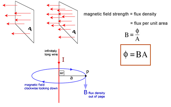
Magnetic flux density (B) is the quantity of magnetic flux (Φ) per unit area (A), measured at right angles to the magnetic field.


The magnetic field can be visualized as magnetic field lines. The field strength corresponds to the density of the field lines. The total number of magnetic field lines penetrating an area is called the magnetic flux Density(D). The unit of the magnetic flux is the tesla meter squared (T · m2, also called the weber and symbolized Wb).


Magnetic flux density (B) is measured in Newton-meters per ampere (Nm/A), also called Tesla (T).


magnetic flux

Comments

Post a Comment

Popular posts from this blog

voltage

Voltage, is is the difference in potential between two points  in an electric field. also called electromotive force. voltage is the   pressure from an electrical circuit’s power source that pushes charged electrons (current).           grater the voltage grater the flow of electric current. Voltage is symbolized by   V or E . The standard unit is the volt. One volt will drive one columb  (6.24 x 10 18 ) charge.such as electronics through a resistance of one ohm. Voltage can be direct or alternating. A direct voltage maintains the same polarity. In an alternating voltage, the polarity reverses direction periodically. The number of complete cycles per second is the frequency which is measured in hertz.

BJT (bipolar junction transistor)

A bipolar junction transistor is a three terminal semiconductor current controlled device with two P-N junctions. The three terminals are emitter(E), base(B) and collector(C). the emitter junction is heavily doped, base is less doped and made very thin and collector terminal is moderately doped. Collector has grater size than emitter and base terminal is thinner than both. (The thinner the base, the stronger the E-C electric field, and the larger the impact of a small current injected into the base. Explained clearly in active mode operation below) emitter terminal is moderate in size. A BJT has two types of transistors: NPN transistor PNP transistor NPN transistor : In an NPN transistor a p-type material is sandwiched between two n-type materials. [gallery ids="979,978" type="rectangular"] PNP transistor : In a PNP transistor a n-type material is sandwiched between two p-type materials. [gallery ids="989,990" type="rectangular"] Oper...

tunnel diode

introduction : A tunnel diode is a highly doped semiconductor device that conducts current by quantum mechanical tunneling. it is also called as esaki diode named after leo esaki who got Nobel  prize in physics for discovering electron tunneling in 1973. Tunneling  Phenomenon: According to classical laws of physics, a particle must have an energy at least equal to the height of a potential-energy barrier if it has to move from one side of the barrier to the other. In other words, energy has to be supplied from some external source so that the electrons on one side of junction climb over the junction barrier to reach the other side. However if the barrier is thin such as in tunnel diode, the Schrodinger equation(Quantum Mechanics) indicates that there is a large probability that an electron will penetrate through the barrier. This will happen without any loss of energy on the part of electron. This quantum mechanical behavior is referred to as tunneling and the high-impurity P-N junctio...